5 minutes
P-N Junction Diode Characteristics(Forward & Reverse)
Aim
The aim of this experiment is to study the forward and reverse characteristics of a P-N junction diode and to determine its cut-in voltage and resistance.
Components Required
| Component Name | Quantity |
|---|---|
| P-N Junction Diode | 1 |
| Resistor | 1 |
| Power Supply | 1 |
| Multimeter | 1 |
| Crocodile Clips | 2 |
Equipments Required
- Oscilloscope
- Connecting wires
Theory
P-N Junction Diode
- A P-N junction diode is a two-terminal device made of a p-type semiconductor material and an n-type semiconductor material joined together. The p-type material has a surplus of holes (positive charge carriers) and the n-type material has a surplus of electrons (negative charge carriers).
- The P-N junction diode is made up of a semiconductor material, such as silicon, that is doped with impurities to create the P and N regions.
- The P region is doped with a material that has an excess of holes, while the N region is doped with a material that has an excess of electrons. This creates a depletion region called as
Barrier Potentialin the middle of the P-N junction, where there is a lack of charge carriers.
Forward Bias
- When a positive voltage is applied to the p-type material, and a negative voltage to the n-type material, the diode is said to be in a forward-biased state.
- In this state, the electric field generated by the applied voltage pushes the holes towards the n-type material and the electrons towards the p-type material. This creates a neutral region at the junction, known as the depletion region, where the concentration of charge carriers is very low. The depletion region acts as a barrier to the flow of current, but the electric field generated by the applied voltage overcomes this barrier and allows current to flow.
- The
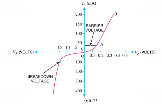
cut-in voltageof a diode is the minimum voltage required to forward-bias the diode and make it conduct. - The forward voltage required to bring the P-N junction diode into the forward-biased state is called the forward voltage drop or the forward voltage threshold.
- This value is around
0.7 VforSi(Silicon)diodes and0.3 VforGe(Germanium)diodes.
Reverse Bias
- On the other hand, when a negative voltage is applied to the p-type material, and a positive voltage to the n-type material, the diode is said to be in a reverse-biased state.
- In this state, the electric field generated by the applied voltage pushes the holes away from the n-type material and the electrons away from the p-type material. This increases the width of the depletion region and makes it more difficult for current to flow. The reverse-biased voltage must be high enough to overcome the built-in potential of the junction and push the majority carriers to the other side of the depletion region.
- The reverse
breakdown voltageis the minimum reverse voltage required to cause breakdown of the diode. - The reverse saturation current is the minimum current that flows through the diode when it is reverse-biased. It is due to the thermal generation of carriers within the depletion region.
Ideality Factor
- The ideality factor, also known as the quality factor, is a parameter that describes the non-ideal behavior of a P-N junction diode. It is the ratio of the actual voltage across the diode to the thermal voltage.
Conclusion
- In conclusion, the forward and reverse characteristics of a P-N junction diode are dependent on the doping levels and the voltage applied across it.
- By understanding these characteristics, we can use P-N junction diodes to build electronic circuits that perform a variety of functions, such as
rectification,voltage regulation, andovervoltage protection.
Procedure
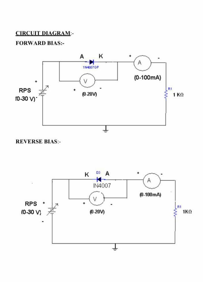
Set up the circuit as shown in the circuit diagram, connecting the P-N junction diode, resistor, power supply, and multimeter as indicated.
Start by applying a small voltage to the diode, gradually increasing it until the diode begins to conduct.
Note down the voltage at which the diode begins to conduct and the current flowing through the diode.
Repeat the above steps for different values of applied voltage, and plot a graph of voltage versus current.
Reverse-bias the diode by reversing the polarity of the applied voltage, and measure the reverse current flowing through the diode.
Repeat the above steps for different values of reverse-biased voltage, and plot a graph of voltage versus reverse current.
Repeat the entire procedure at least two more times to obtain more accurate results.
Calculate the cut-in voltage and resistance of the diode from the plots obtained.
Compare the calculated values with the expected values for the diode.
Observe the waveform of the voltage and current on the oscilloscope.
Record the observations and the results of the experiment in a report.
Clean up the circuit and return all components to their proper storage location.
Repeat the experiment with different diodes and compare the results.
Analyze the effect of temperature on the forward and reverse characteristics of the diode.
Investigate the effect of reverse-biased voltage on the breakdown voltage of the diode.
Determine the effect of diode capacitance on the waveform of voltage and current in the circuit.
Circuit Diagram 👇🏻
Forward & Reverse Characteristics Graph 👇🏻
Precautions
- Ensure that the circuit connections are secure and tight to avoid any loose connections.
- Use a
LOWvoltage power supply to avoid damaging the diode. - Use protective equipment, such as safety glasses, when working with high voltage.
AVOIDtouching any live wires or components in the circuit.- Make sure to
DISCHARGEany stored charge in the circuit before touching it.
Summary
In this experiment, the forward and reverse characteristics of a P-N junction diode were studied by measuring the current flowing through the diode for different values of applied voltage. The cut-in voltage and resistance of the diode were calculated from the obtained results and compared with the expected values.
Conclusion
The forward and reverse characteristics of a P-N junction diode were experimentally determined and analyzed. The results showed the behavior of the diode in both forward and reverse bias conditions, and demonstrated the importance of the P-N junction in rectifying AC signals. The experiment also emphasized the importance of following proper precautions and safety measures when working with electrical circuits.
1011 Words
2023-01-28 16:04